Abstract: Semiconductor lasers are the core components in the field of optical fiber communication, laser display, and gas detection, and have received extensive attention from scientists and technicians all over the world. In the production and development of semiconductor lasers, a large number of PIV tests are performed on semiconductor laser chips. The article introduces some applications of digital source meter B2900A in semiconductor laser testing for your reference.
Semiconductor lasers are the core components in the field of optical fiber communication, laser display, and gas detection, and have received extensive attention from scientists and technicians all over the world. In the production and development of semiconductor lasers, the measurement of the optical characteristics of the laser is particularly important. It is a key step in controlling the stability of the laser preparation process and the reliability of the laser performance.
Semiconductor lasers are semiconductor photoelectric conversion devices. As shown in FIG. 1, the semiconductor laser is composed of multiple layers of material. The bottom electrode includes a back electrode, a substrate, a lower light confinement layer, a lower wave guide layer, an active layer, an upper wave guide layer, an upper confinement layer, and an upper electrode. Different layers consist of different epitaxial materials. The layered structure is such that 1) the complex emission of carriers (electrons, holes) is injected, and 2) the photons are laterally limited to form the optical waveguide. The epitaxially completed layered structure is subjected to an etching process to form a ridge waveguide and a contact electrode is prepared on the ridge waveguide. The purpose of such a ridge waveguide is 1) to limit the lateral diffusion of the current, and 2) to form the photon's lateral waveguide. The prepared wafer was subjected to cleaving, coating, welding, pressure welding, and the like to obtain a laser to be measured, as shown in FIG. When a current is injected into the laser electrode, electrons and holes on both sides of the laser PN junction inflow into the active region in a large amount. In the active region, the electron hole pairs recombine to generate a large number of photons. The photons are axially directed by the waveguide. Propagation: At the end of the laser, reflected light forms a lasing condition, and transmitted light is a laser output from the laser. The operating characteristics of the laser are mainly reflected in 1) PN junction characteristics, series resistance, 2) laser lasing threshold, and laser slope efficiency. These characteristics determine the laser output power PO, power conversion efficiency ηP, working life and other properties. PIV measurement methods are often used to obtain these important parameters during production and scientific research.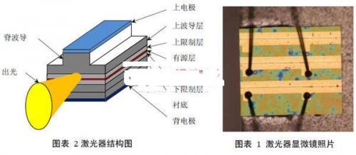
The PIV characteristic of the semiconductor laser is the response characteristic of the laser output power P and the laser diode voltage V when the current I is injected into the laser. Unlike ordinary PN junction diodes and other two-terminal devices, semiconductor laser PIV testing not only measures the voltage-current (VI) characteristics of the laser, it is important to simultaneously perform the power-current (PI) characteristics of the laser. Therefore, semiconductor laser PIV test systems include precision current sources, voltmeters, power meters, and software components responsible for control, inter-instrument communication, data acquisition, and processing. The traditional PIV test system consists of a discrete current source (integrated with a voltmeter), a galvanometer, and control software. The current source is used to provide the laser injection current and the measurement voltage. The galvanometer is connected to the integrating sphere for measuring the laser power. The current source and the galvanometer are connected with the software through the GPIB port to complete the tasks of measurement triggering and data transmission.
The complex PIV test system has many problems, including 1) the measurement speed is not high, the number of points measured per unit of time is small, and the measurement time is increased; 2) the stability of the system is poor, and data transmission blocking occurs between instruments connected by the GPIB port. The problem is that the system is prone to defects; 3) The controllability of the system is poor, the measurement speed, the number of scanning points, and the scanning method cannot be adjusted according to the measurement requirements. In a large number of semiconductor laser optoelectronic test processes, conventional PIV test systems have experienced problems of low efficiency, reliability, and poor controllability.
B2900A integrated PIV test system B2900A integrated PIV test system (referred to as the integrated PIV system) is designed and built by the experimental group. The PIV test is performed using a precision source measurement unit SMU and an integrating sphere detector combination system. The system has a simple structure, high accuracy, good reliability, and high speed. It also increases the production efficiency, increases the test accuracy and reliability, and reduces the cost of a large number of tests. The integrated PIV system is composed of the B2900A dual-channel precision source measurement unit SMU, integrating sphere, fixture and software. One channel CH1 of the B2900A is used as the current source of the laser to measure the voltage V of the laser at the same time. The lasing light of the LD is coupled into the integrating sphere, converted into photocurrent by the integrating sphere detector into another channel CH2 of the B2900A, and the photocurrent measured by the B2900ACH2 is multiplied by the power conversion coefficient of the integrating sphere detector to obtain the output of the laser. power. The B2900A is connected to the PIV measurement software via a USB port for measurement control and data acquisition. Figure 3 shows the experimental connection. During the measurement, the parameters of the test are set by the PIV test software, and the PIV measurement is triggered simultaneously in CH1 and CH2. The data is returned to the software in real time through the USB port. Through the software interface, the dynamic characteristics of the laser can be observed in real time. At the same time, the characteristic parameters of each laser can be quickly analyzed based on software measurement data, including forward voltage drop VF, optical power PO, threshold current Ith, and inflection point parameters Ikink.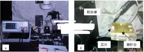
The integrated PIV system highlights superior performance such as ease of operation, high accuracy, high efficiency, and high reliability during a large number of laser PIV tests. All test parameters of the laser can be easily set on the software interface, including current source voltage switching, DC pulse switching, current range, limit voltage, scan mode, scan points, scan time, and speed. This makes it easy to adjust parameters between different measurement conditions. Second, the current measurement accuracy of the B2900A precision source measurement unit can reach 0.1nA. In the high-resistance semi-insulating structure (107~8Ω), the resistance value of the high-resistance structure can be accurately measured with a small driving voltage (<1V). At the same time, the power of the laser is measured synchronously with the voltage and current without external coordinated triggering. When scanning measurement, more than 400 points can be measured within 8 seconds.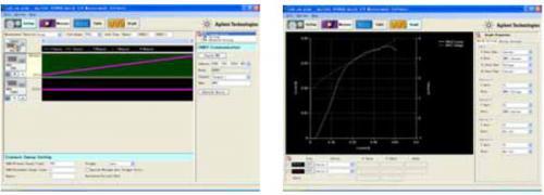
The expandability of the integrated PIV system is also an outstanding advantage in its application in the research and development of semiconductor lasers. The hardware part of the integrated PIV system, including the B2900A precision measurement unit, the measurement platform, is connected to the computer via a GPIB or USB port. Therefore, the hardware part of the integrated PIV system can be used with the test software program written by the user through the National Instruments and other software platforms to complete the more complex measurement tasks required by the user.
In the production and development of semiconductor lasers, a large number of PIV tests are performed on semiconductor laser chips. Compared with the traditional discrete and complex PIV test system, the PIV test system integrated with the B2900A precision measurement unit has the advantages of simple system structure, convenient operation, high precision, high reliability, and rapid measurement, which greatly reduces the operation of laser chip PIV performance measurement. Cost, time cost, and increased flexibility of PIV measurements. B2900A precision measurement unit will be widely used in semiconductor laser production and scientific research and other fields.
Some of the key things that you have to consider when buying a heated car seat include the heating panels, comfy level, ease of installation, adjustable temperature, and price just to mention a few.


12V Heated Pads,Seat Oxygen Ventilator,Homemade Seat Warmer,Carbon Fiber Car Seat Heater
JiLin Province Debang Auto Electric Co.,Ltd. , https://www.dbheatedpads.com